What’s this blog about?
As part of my effort to build my own computer, I’ve been learning about Random Access Memory (RAM) recently, and there’s a lot to learn here! Who knew that there’s more to a RAM than what meets the eye?
Anyway, since there’s too many things to learn, I need to record what I learned (much like my learning process with high frequency PCB) so it would be easier for me to review in the future.
Introduction
DDR3 DRAMs follows a set of rules known as DDR3 SDRAM standard set by the Joint Electron Device Engineering Council (JEDEC), which can be accessed here.
While reading through the entire 200-page manual is definitely the best approach, I find doing so incredibly exhausting. Therefore, I’d like to try a different approach: learning by looking at a reference board and read the DDR3 SDRAM standard (partially) while reading the specific datasheet of the DRAM used by the reference board.
Therefore, although this blog is themed as DDR3, I am discussing a specific implementation of DDR3 SDRAM standard, not the standard itself.
For the reference board, I chose Nanopi NEO since it uses Allwinner H3 SoC, which I plan to use in my board as well. Since Nanopi NEO uses Samsung’s K4B2G1646B-HCH9, we need to grab its datasheet as well from this link.
DDR3 at a glance
As mentioned previously, this blog will be based off Samsung’s K4B2G1646B-HCH9, specifically the 128x16 variant. I’ll try to mention if a specific detail is just specific to the chip and not a part of the DDR3 SDRAM standard, but no guarantees :).
Anyway, let’s continue.
DDR3 Architecture: banks
Internally, DDR3 is divided into 8 cores, also known as banks. Each bank is further divided into rows (accessed with 14 bits address, resulting in a total of 16,384 rows) and columns (accessed with 10 bits address, resulting in a total of 1,024 columns), with each address storing a word of data (16 bits in our case).
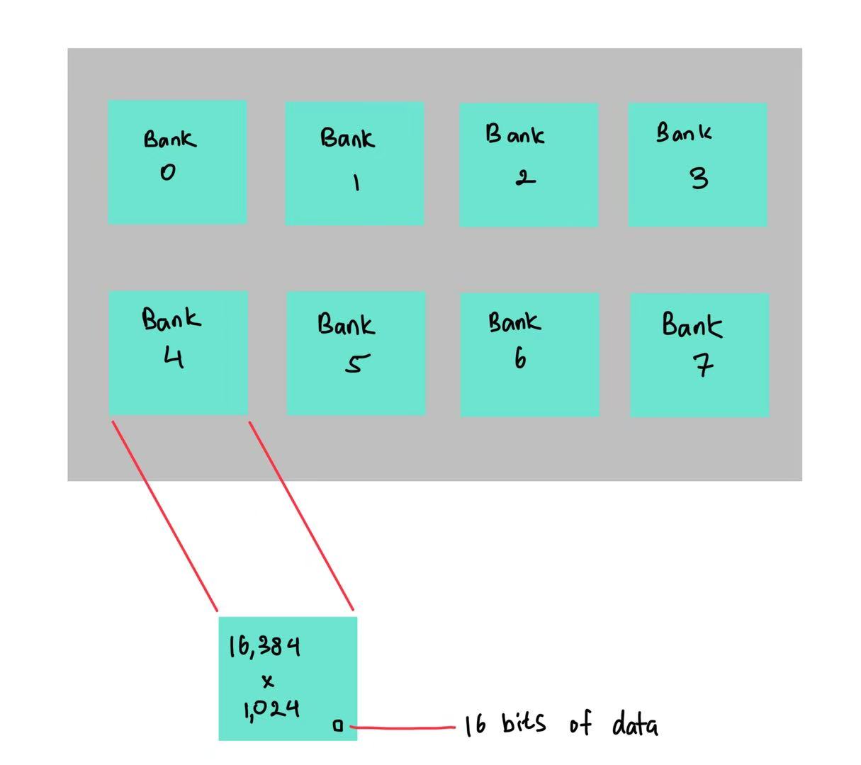
FYI, the number of rows & columns mentioned above is specific to the chip I am using.
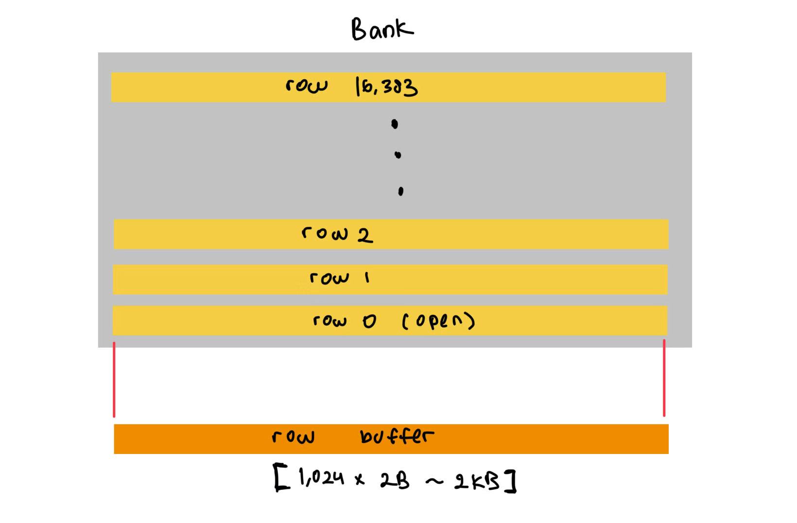
Why is this important? Well, each bank has its own row buffer (a temporary register/memory). Everytime READ / WRITE command is issued, data must go through this buffer. Think of it as a checkpoint for data transfers.
As the name implies, row buffer can only expose one row at a time (When a row is exposed, the row is said to be ACTIVATE [d] ) and if we want to read/write data from/to a different row, we must first PRECHARGE (deactivate) the current row and ACTIVATE (activate) the desired row.
Since there are time penalties when we deactivate/activate rows, we ideally want to access data in the same row as frequently as possible before we deactivate said row. Luckily, thanks to the principle of localization, we generally don’t have to worry about it (although it would help if we keep this in mind when programming our software).
But how much data can we access at a given time?
Well, we know that a bank contains 1,024 columns, with each address location containing 16 bits, or 2 bytes of data. Therefore, we get 1,024 x 2 = 2,048 ~ 2KB of data. The amount of data we can access at a given time is also known as Page size (not to be confused with Page from Operating Systems, which is a software concept).
Mode register
Our DRAM has set of registers known as the mode register. There are four of them, and they are responsible for the following:
- MR0: burst length (BL8), CAS latency (CL), DLL reset, write recovery (tWR).
- MR1: ODT.
- MR2: CAS write latency (CWL), write-ODT (RTT_WR), temperature features.
- MR3: test/MPR stuff.
To better understand how these registers are set on Allwinner H3, let’s look at Allwinner H3’s firmware, specifically at this code chunk:
/* set mode register */
writel(0x1c70, &mctl_ctl->mr[0]);	/* CL=11, WR=12 */
writel(0x40, &mctl_ctl->mr[1]);
writel(0x18, &mctl_ctl->mr[2]);		/* CWL=8 */
writel(0x0, &mctl_ctl->mr[3]);
We won’t be discussing this code chunk in detail for now; however, we’ll get to them very soon!
DRAM pins
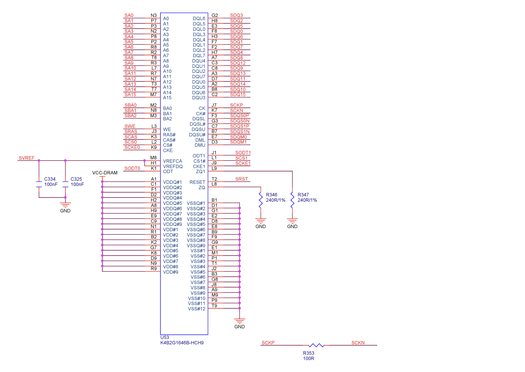
Now that we know the basic architecture of my chosen DRAM, let’s familiarize ourselves with its pinouts. Looking at Nanopi Neo’s schematics, here’s the pinout of the DRAM:
Power pins
I think this one is quite simple: VDDQ1-9 & VDD1-9 are connected to the power supply, while VSSQ1-9 & VSS1-12 are connected to ground.
Since these lines don’t carry signals, we don’t have to worry about length matching & to a lesser extent, impedance matching (we can ignore it altogether but we will waste power). However, since my goal is just to get a functional computer, I won’t pay much attention to these trace lines, except for the fact that it must supply 1.5 V to the DRAM. Additionally, the trace must be designed to ensure that it can withstand 1.5 W of power, which implies that its maximum current is 1 A.
Data pins
-
DQ pins
In total, there are 16DQpins, with 8 being upper byte (DQU) and the other 8 being the lower byte (DQL). -
DQS pins
There are fourDQSpins, two for the upper byte (DQSU&DQSU#) and two for the lower byte (DQSL&DQSL#). Their job is to latch the state of theDQpins. -
DM pins
There are twoDMpins,DMU&DML. Their job is to mask the bits of theDQlines. -
VREFDQ pin
This is a reference pin used by the data. Normally set to half the supply voltage.
It is worth noting that, all of the data pins have built-in On-Die Termination (ODT), meaning we won’t need to add terminating resistors to these pins. Instead, we only need to program the firmware so we have the desired impedance at each pins and the SoC’s DRAM controller will send signals to the ODT pin of the DRAM chip.
To know the exact impedance, recall this code chunk mentioned earlier, which is used to set the mode register:
/* set mode register */
writel(0x1c70, &mctl_ctl->mr[0]);	/* CL=11, WR=12 */
writel(0x40, &mctl_ctl->mr[1]);
writel(0x18, &mctl_ctl->mr[2]);		/* CWL=8 */
writel(0x0, &mctl_ctl->mr[3]);
From here, we can see that bit 9, 6, & 2 of MR1 are set to 0, 1, 0 respectively (from 0x40, which is 0b0-001-000-000). Looking at Samsung’s datasheet:
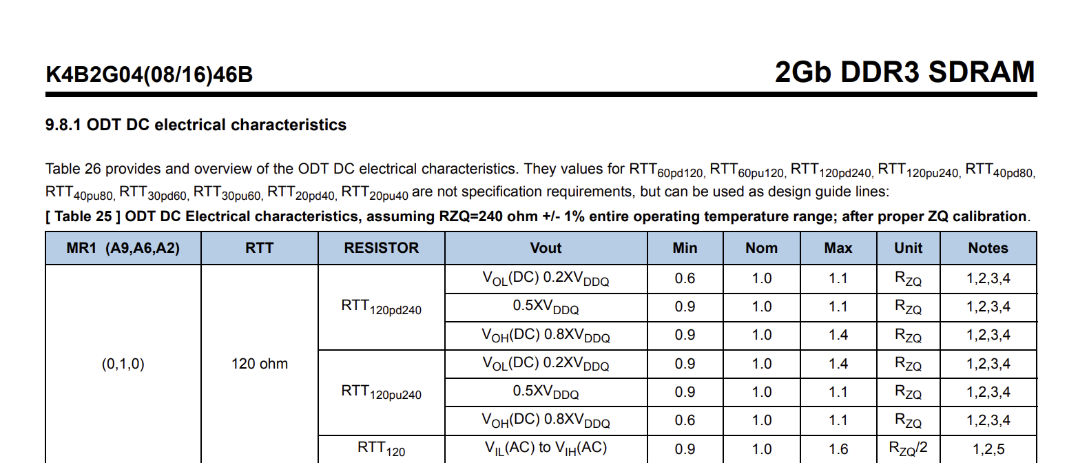
We can see that our data pins are terminated with 120 ohms terminating resistors. Therefore, we need to keep this in mind when deciding on our trace width.
Control pins
-
CS# pin
This pin is used to select/deselect the DRAM chip. Active low, and is controlled by theDRAM controller. -
RAS#, CAS#, WE# pins
These three pins, when used in certain combinations, result in different behaviors of the DRAM chip. Here’s a table outlining the behavior of each combination (table generated by ChatGPT because I’m lazy):
| RAS# | CAS# | WE# | Command (Name) | Notes |
|---|---|---|---|---|
| 1 | 1 | 1 | NOP | Ignore CA for this CK; keeps pipeline alive. (If CS#=1 → DESELECT.) |
| 0 | 1 | 1 | ACTIVATE | BA[2:0] = bank, A[13:0] = ROW (for 2 Gb x16). Wait tRCD before RD/WR. |
| 1 | 0 | 1 | READ / READ w/ AP | BA[2:0] = bank, A[9:0] = COLUMN; A10 = 1 → Auto-Precharge; A12 = burst-length on-the-fly (BL8/BC4). Data out after CL. |
| 1 | 0 | 0 | WRITE / WRITE w/ AP | BA[2:0] = bank, A[9:0] = COLUMN; A10 = 1 → Auto-Precharge; A12 = BL OTF. Controller drives DQ/DQS; obey WL and tWR before precharge. |
| 0 | 1 | 0 | PRECHARGE / PRECHARGE ALL | A10 = 0 → precharge bank in BA; A10 = 1 → precharge all banks. Must meet tRP. |
| 0 | 0 | 1 | AUTO REFRESH | Address don’t care. Must meet tRFC before next ACT. |
| 0 | 0 | 0 | MODE REGISTER SET (MR0–MR3) | BA selects MR (000→MR0…011→MR3). A[15:0] carry MR bitfields (BL, CL, WR, DLL, ODT, CWL, MPR, etc.). Observe tMRD before next command. |
-
CK/CK# pins
These are the clock pins. They are differential pairs, and must be terminated with a 100 ohms differential terminating resistor. -
CKE pin
Used for initialization purposes. I won’t cover this in detail. -
RESET# pin
It is used for, well, resetting the DRAM chip. -
VREFCA pin
This is a reference pin used by the control pins (CApins). Normally set to half the supply voltage.
Address pins
-
BA pins
Used to specify the bank we want to access. Since there are 8 banks, there are three bank pins (BA0-2). -
SA pins
The pins used to specify the row/column, depending on the state of other pins. Specifically, during ACTIVATE, they carry the row address. During READ/WRITE, they carry the column address and other options.
Miscellaneous pins
-
ODT pin
Used for, well, ODT purposes. -
ZQ pin
Used for callibration purposes. Attach a240 ohmsresistor to it.
DRAM initialization
I’m not sure if this will be needed, but I’ve asked ChatGPT on the workflow of DRAM initialization and this is what it came up with:
-
Boot ROM jumps into SPL (tiny first stage running from SRAM).
-
Clocks on: SPL sets the DDR PLL to your CONFIG_DRAM_CLK (e.g., 408 MHz → DDR-816).
-
Program the controller: tell it bus width (×16), ranks, timings in cycles, address map, and ODT policy.
-
Tell the DRAM who it is: issue MRS writes:
- MR0 (BL/CL/…),
- MR1 (e.g., RTT_NOM = 120 Ω),
- MR2 (e.g., CWL = 6 or 7, optional RTT_WR),
- then ZQ calibration so the DRAM trims its drivers/ODT to real silicon (uses the external 240 Ω RZQ).
- Train the PHY (calibrate delays so timing lines up on your PCB):
- Write leveling: adjust each lane’s DQS so the DRAM sees it aligned to CK (write path).
- Read gate / read leveling: find where returning DQS sits and center the read eye on DQ (read path).
- Optionally small per-bit deskew if supported.
- The discovered delays are written into the PHY lane registers.
- Width confirm / auto-detect: if upper lanes (2/3) don’t train (because they’re not wired), SPL:
- marks bus width = 16 in the controller,
- disables those lanes in the PHY,
- proceeds with lanes 0/1 only.
- Done: DRAM now works; SPL loads U-Boot proper into RAM and jumps.
Again, I’m not sure if I will ever need this when designing my own computer, but I’ll just list it here for now for future reference (I didn’t even bother paraphrasing it because frankly, I haven’t studied it yet :D).
Some more concepts to cover
Now that we’re already familiar with the DRAM pins, I think now would be a good time to discuss another key concept in DDR3, which is setup/hold time.
I found a good diagram from YouTube:
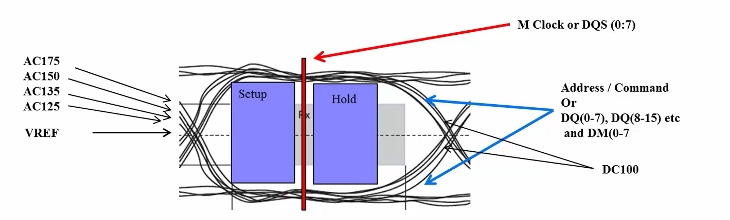
So what’s this all about? Well, when we want to write a data, we set relevant pins to 0 or 1, then when the strobe pins are activated, the data will get recorded, much like us humans taking a picture.
However, just like us humans, we must be ready with our chosen pose before the cameraman snaps the picture. The same is true for DDR3, and it is called setup time.
Additionally, there is also a time where the state of the pin must be kept after the strobe pins activate. This is called the hold time.
But at what voltage levels must the signal be for the duration of setup/hold time?
Well, that’s what those ACXXX are. ACXXX means that the signal must be VREF + XXX (if signal is HIGH) at least for a certain amount of time before the strobe signal is active (or VREF - XXX if the signal is LOW).
For hold, we use DC100.
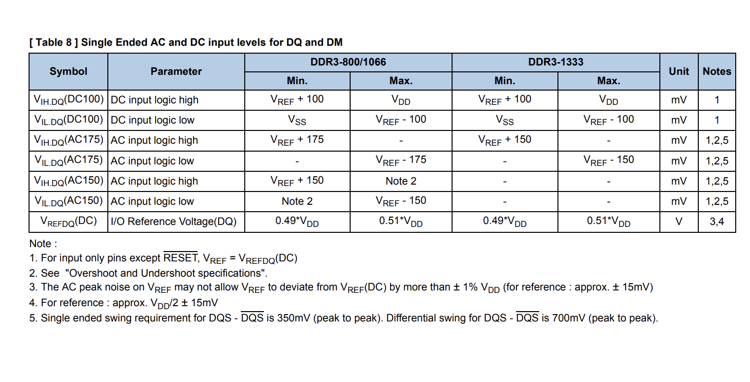
Let’s see what are the setup & hold times for our Samsung chip. First, let’s check the voltage thresholds on the datasheet:
And finally, the setup & hold times:
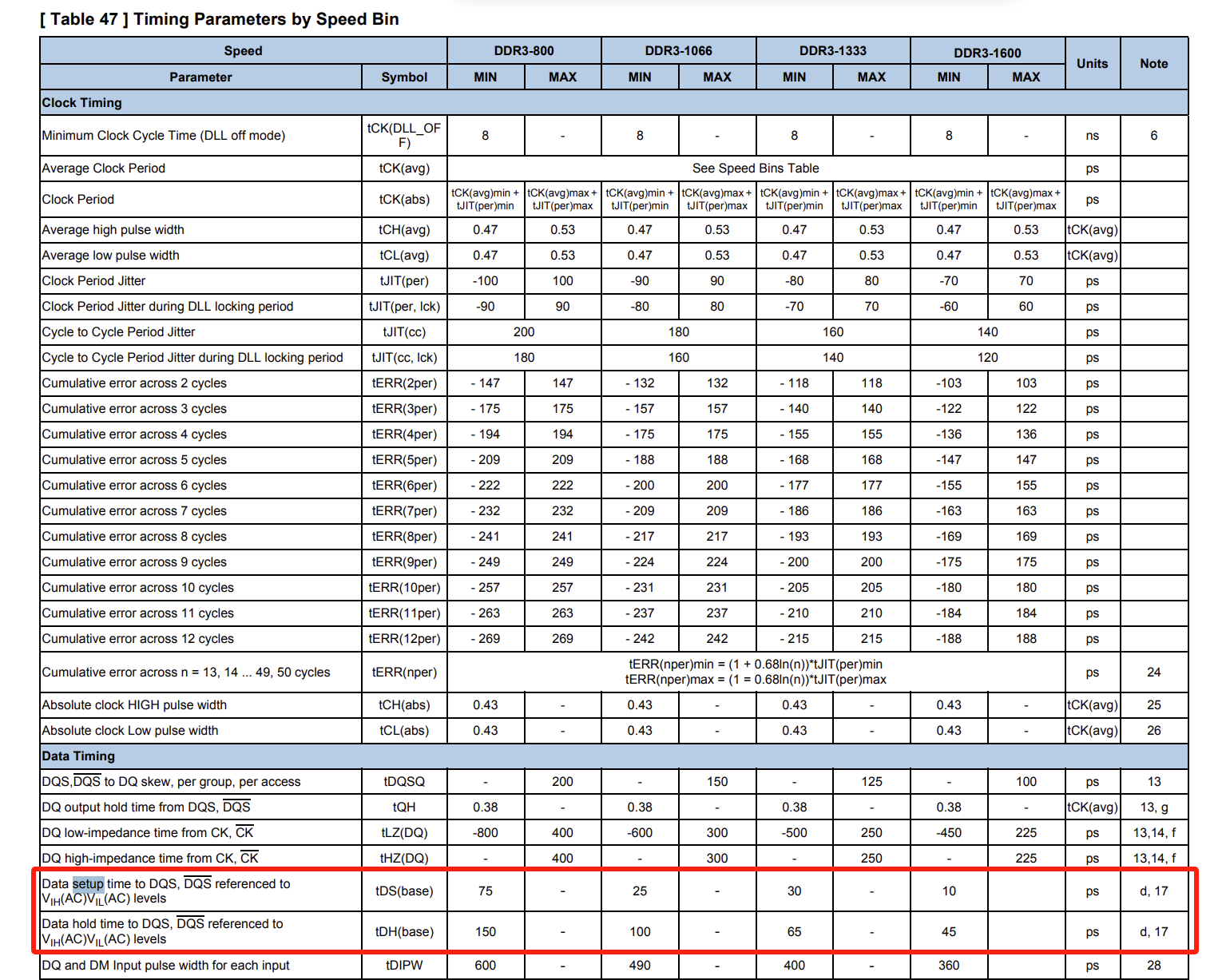
Here, if we’re using DDR3-1333, then the setup time is 30 ps, while the hold time is 65 ps. Additionally, I’m not sure which AC level to use, but let’s assume a worst case of AC175 for DDR3-1333.
Anyway, it won’t matter for the PCB design. I’m mentioning it just for completeness.
PCB trace constraints
Next, we need to consider our PCB constraints. To do this, we need to obtain the PCB design guide from the manufacturer.
It was hard to find for Allwinner H3, but I finally found it here.
I won’t be showing screenshots since I need Allwinner’s permission to redistribute the PCB design guide, but you can just view it on the link I provided.
Trace impedance
From the PCB stackup, we can see that it is recommended to aim for 50 ohms for single ended trace and 100 ohms for differential.
I find this information conflicting - In the u-boot firmware (written by Allwinner), we have seen that the Mode register has been set in a way that results in the DRAM pins (some of them) to have 120 ohms ODT.
Why not 40 ohms or 60 ohms?
That’s what I’ve been wondering too. When I asked ChatGPT, I couldn’t get a satisfying answer. However, here’s its paraphrased reply:
“We use 120 ohms ODT to reduce current draw and therefore saves power. For short traces, the reflection won’t have much of an impact anyway”.
Clearances
Here’s a list of the clearance requirements:
- Line-to-line: >= 8 mil (outer & inner).
- Diff pair - other nets: >= 15 mil.
- Power/ground - other nets: >= 15 mil.
- VREF - any net: >= 15 mil (keep it quiet).
- BGA escape area minimums: line-to-line 4 mil, line-to-pad 4 mil, line-to-via 4 mil.
Length matching
And here’s the list for the length mismatch tolerance:
- Within each byte lane: match DQ0–7 to DQS0/DQS0# (and DQ8–15 to DQS1/DQS1#) with <= 50 mil tolerance; via counts identical within the lane.
- DQSx - CK/CK#: <= 800 mil difference.
- CA group (A/BA/Cmd/Ctrl) - CK: <= 600 mil difference.
- Intra-pair (diff): DQSx vs DQSx# <= 10 mil, CK vs CK# <= 10 mil.
Length matching (conversion)
If we assume roughly that FR-4 ~ 6.5 ps/mm and 1 mm ≈ 39.37 mil:
- 0 mil ~ 0.254 mm ~ 1.7 ps
- 50 mil ~ 1.27 mm ~ 8.3 ps
- 100 mil ~ 2.54 mm ~ 16.5 ps
- 600 mil ~ 15.24 mm ~ 99 ps
- 800 mil ~ 20.32 mm ~ 132 ps
Conclusion
DRAM is the most complex subsystem that I will design, and the most expensive too. Therefore, I need to make sure everything is right before I order my PCB, so as to not waste any money.
As for now, I think I’ve had a good understanding on what I have to do on the DRAM subsystem, except for the 50 ohms & 120 ohms contradiction. I’ll update this blog when I find a good answer, but until then, take care!