What’s this blog about?
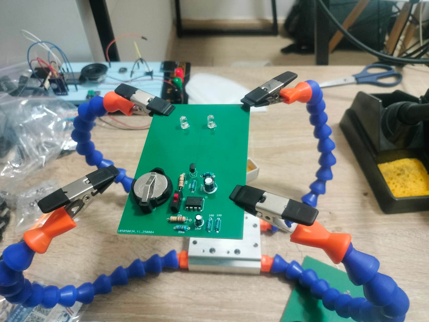
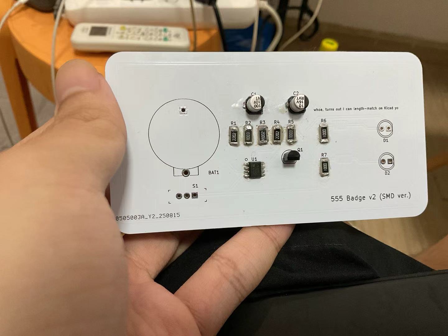
I spent much of my summer break (while being unemployed) learning PCB design. Specifically, I’ve been following Shawn Hymel’s Kicad tutorials on YouTube and made some simple circuits (Please don’t judge, I know I’m still shit, especially at SMD soldering):
Anyway, while my soldering skills definitely needs improvement (or maybe I need to buy a hot air gun instead), I think I’m quite comfortable with Kicad already. Therefore, I began to learn about high frequency PCB design, to know what do I need to keep in mind when designing my own computer, as well as finding out if Kicad is usable for high frequency design (I was concerned with its viability since most people use Altium).
Over the weeks, I’ve learned quite a few things, and I feel that I need to record them somewhere so it would be easy for me in the future to review; hence this blog.
The problem with high frequency signals
You may wonder, if I can already design my own PCB, then what’s the problem? Well, in high frequency, signals oscillates so fast that it emits non-negligible electric & magnetic fields. Given that signals that create these fields are oscillating, the values of these fields oscillate as well. This, in turn, can cause current to be induced to nearby traces, causing signal integrity issues.
Another issue is that, since we’re dealing with high-performant components operating at MHz or even GHz frequencies, the margin of error is so small (in the ps range) that the time it takes for an electron to travel from one end to another can no longer be ignored, hence we need to pay a very close attention to the length of our PCB traces.
Critical length
As implied earlier, electrons travel at finite speed. Specifically,
$$ v_{\text{propagation}} = \frac{c}{\sqrt{\varepsilon_r}} $$
Where:
$$ v_{\text{propagation}} = \text{speed of propagation} $$
$$ c = \text{speed of light in vacuum} $$
$$ \varepsilon_r = \text{relative permittivity of the medium} $$
Given this, if the length of the trace is too long, then it will take a non-negligible amount of time for a signal to travel over the trace, and with margin of error in the ps regime, it could be problematic.
The value of the length where it becomes problematic is known as the critical length, at which point we need to treat the trace as transmission line.
Specifically, the issue is as follows: if there is an impedance mismatch (discussed further in a later section), then when a signal reaches the point where the mismatch occurs, that signal will be reflected back, interfering with the next incoming signal.
Now, if the trace is short, then there won’t be any problem because the signal & its reflection traverse the entire trace before the next signal comes in.
The reflection will still interfere with the original signal. However, since we’re dealing with digital signals, we don’t need to worry about interference, since they will interfere constructively.
However, with high speed circuits (such as DDR3), the interval between two signals can be as low as 200ps. Therefore, proper measures should be taken to prevent it from causing problems, such as adding terminating resistors or making the traces short (below its critical length).
As a rule of thumb, the critical length is simply the propagation velocity multiplied by time delay (which can be anything. For example, it can be the signal rise time) divided by two:
$$ L_{\text{critical}} = \frac{v_{\text{propagation}} * T}{2} $$
Or, we can simply express it as such:
$$ L_{\text{critical}} = \frac{T}{2 * t_{\text{propagation delay}}} $$
Let’s play around with some numbers to get a feel for the problem:
Suppose you want to route a DDR3-800 trace. Specifically, you want to calculate the critical length of one of the data lines. If we assume that the edge skew is 200 ps using the FR-4 stripline (7 ps/mm propagation delay), we get:
$$ L_{\text{critical}} = \frac{200}{2 * 7} $$
$$ L_{\text{critical}} = 14.2 mm $$
That means our trace will have to be less than 14.2 mm, or 1.42 cm in length!
I remember having issues understanding critical length. Well, here’s how I think of it using the previous example:
“Our DDR3-800 DRAM ‘blinks’ once every 200ps. Therefore, if our signal can make a round trip around the trace within 200ps, then the DRAM won’t notice.”
Helpful link(s): Link 1
Cross Talk
As mentioned before, oscillating signals emits changing magnetic & electric fields. These fields, in turn, can induce current to nearby wires (or trace in our case), and, the higher the frequency, the greater the induced current will be. When this happens, signal from one trace can seem to “jump” to another trace, interfering with the signal on that other trace. This phenomenon is known as cross talk.
I know that electromagnetism is complicated, so think of it this way: a capacitor’s impedance is given as:
$$ Z_C = \frac{1}{j*2\pi fC} $$
where:
$$ f = \text{frequency of the signal} $$
$$ C = \text{Capacitance} $$
$$ j = \text{imaginary number} $$
The impedance is inversely proportional to the frequency. In other words, at high frequency, capacitors act as short circuits.
Why mention capacitors?
Well, capacitors are just two conductors separated with an insulator, same with two traces close together.
There are complicated theories & formulaes with relation to cross talk, however, I’ve been told that a good rule of thumb is that trace gap must be at least three times the distance of the signal trace with the nearest ground plane.
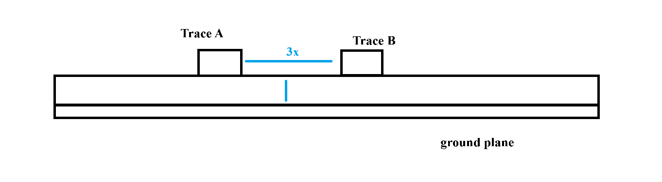
Following this, one good way to minimize cross talk is to use thinner dielectric materials. Just make sure your manufacturer can manufacture your design.
Helpful link(s): Link 1
Return Path
When there’s a potential difference, then an electric field will be induced. Because there’s a difference in voltage between our signal trace & ground plane, our trace is no exception:
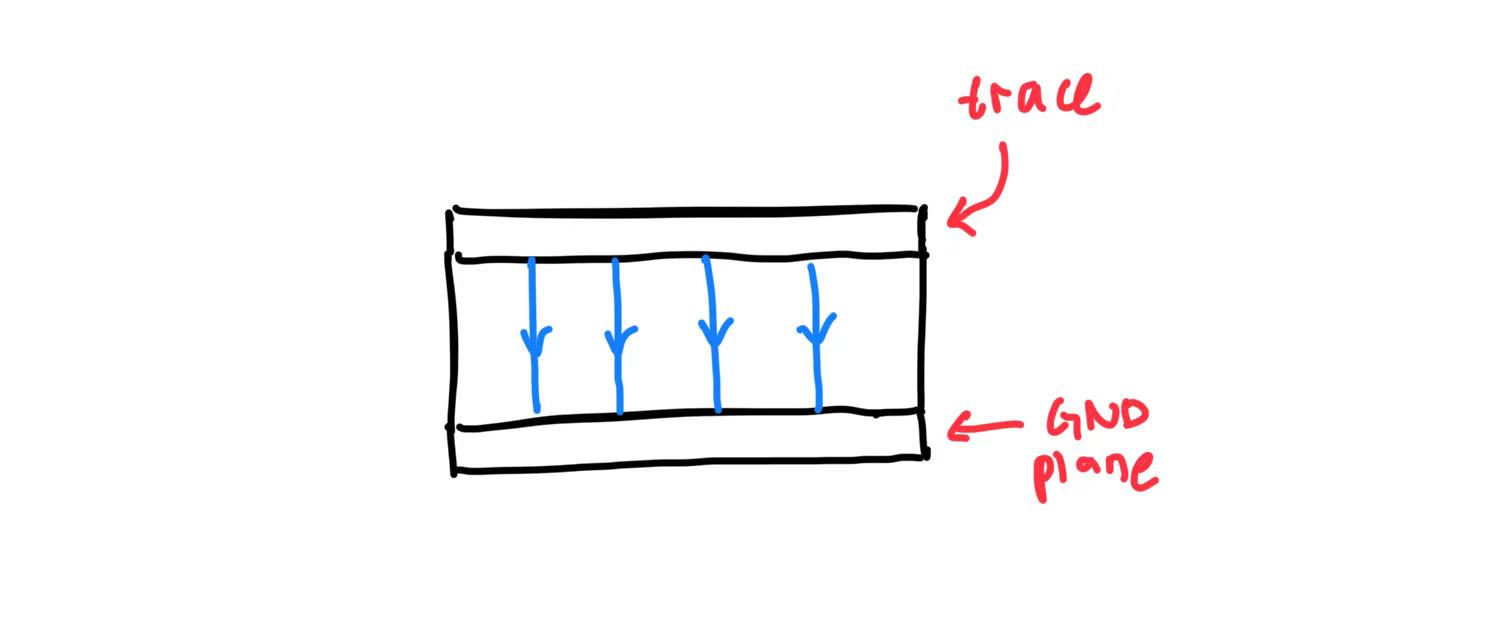
In other words, signals induce electric fields to the ground plane, kind of like shadows. To make sure that our signal won’t interfere with other circuitry on the board, aside from the three-times-trace-width rule, it is also our job to make sure that we know where our current’s return path is.
I think Ferenec made a good video visualizing return path (link at the end of this section). Here’s a screenshot of his visualization:
I think you need simulators to make sure that your circuit has predictable return path. However, one good rule I learned from watching multiple videos is, whenever you change layer (for example from layer 1 to layer 4) using vias, add guard vias connecting the nearest ground planes (for example, if layer 1’s closest ground plane is layer 2, while layer 4’s closest ground plane is layer 3, then you use the guard vias to connect layer 2 & layer 3).
Helpful link(s): Link 1
Impedance & Length Matching
I put them together since they are somewhat similar, but let’s talk about them one by one.
First, impedance matching.
Have you ever tied a rope to a wall, and then wave the free end of the rope? What happens?
The wave will travel across the rope. However, when it reaches the wall, it will get reflected back because reflection occurs when a wave crosses a different medium.
Same goes with signals: the “medium” is impedance. If you’re wondering why exactly, TBH I’m not sure myself. However, I think just knowing that reflections due to impedance mismatch exists is enough for my case.
To mitigate this, we have two options:
- Make sure the entire path a signal takes has uniform impedance. We can do this by modifying trace width to values specified by online calculators.
- Add resistors (called
terminating resistors) to absord the reflections.
Next, length matching.
As mentioned before, signals travel at finite speed. This poses a problem when we want to send data in parallel (For example, K4B2G1646B-HCF7 DRAM has 16 data lines); and to mitigate this, we must ensure that the lengths of our data traces match with one another, at least within an allowable margin as specified on the datasheet of the DRAM you’re working with.
To mitigate this, we add curly lines (meanders) to the shorter trace so that the shorter traces will have their trace lengths match that of the longer ones.
Luckily, you can do this with Kicad: just choose a trace, and enter the target length. Kicad will add meanders for you.
Helpful Link(s): Link 1, Link 2, Link 3
Differential pairs
To be fair, I never expected differential pairs to be quite complicated for PCB design. I have nothing to say here for now, but I’ve been watching some videos, and I find Phil’s video to be the most helpful.
Helpful Link(s): Link 1
Conclusion
I’ve still got a long way to go for my computer to come to life. However, I think so far, high frequency design is more tedious than it is hard (at least the theory).
With that said, I’ll take a break from learning the theory of PCB design and try to get my hands dirty on soldering, specifically SMD soldering.
But I won’t take a break from hardware entirely though - I plan on learning my chosen DRAM (K4B2G1646B-HCF7) next!
Lastly, I’m happy to report that so far, there’s nothing stopping me from using Kicad for high frequency PCB design!